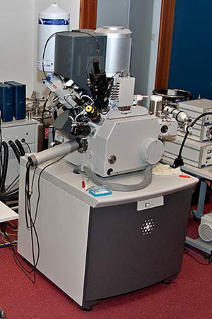
Nova 600 NanoLab
Electron Optics
- Field Emission-SEM column
- Resolution at optimum WD (High-vacuum)
– 1.0 nm at 15 kV (TLD-SE)
– 1.8 nm at 1 kV (TLD-SE)
– 0.8 nm at 30 kV (STEM) - Accelerating voltage: 200 V – 30 kV
- Probe current: 0.3 pA – 22 nA continuously adjustable
- Max. horizontal field width: 3.9 mm at 5 mm WD (corresponds to 30 x minimum magnification in quad view)
Imaging
- In-lens SE detector (TLD-SE)
- In-lens BSE detector (TLD-BSE)
- Everhardt-Thornley SED
- IR-CCD
- TV-rate Solid-State BSED
- TV-rate low vacuum Solid-State BSED (GAD)
- STEM detector
3rd party accessories
- Oxford EDS
- EBSD 3D
- Nanomanipulator
- Lithography systems